Posts

Chemical structure and emission performance of double-borylation ν-DABNA OLED materials developed by Kyoto University and JNC

Kyoto University-JNC joint research team innovates next-generation deep blue OLED materials with new ‘(Double Borylation)’ technology

A joint research team led by Professor Takuji Hatakeyama from the Department of Chemistry at Kyoto University, in collaboration with JNC Co., Ltd., has developed a novel ‘Double Borylation’ synthetic strategy and successfully realized a world-leading pure Deep Blue OLED emitting material. This achievement was published in the international journal Nature Communications (October 2025, DOI: 10.1038/s41467-025-63908-y) and is anticipated to be a core technology for next-generation displays such as high-resolution micro-OLEDs.

Among the three primary colors (RGB) for OLEDs, the ‘Deep Blue’ region is known to be the most challenging to achieve. This is because producing a deeper blue color leads to increasingly unstable charge recombination, resulting in reduced efficiency and shortened lifetime. To address this issue, Professor Hatakeyama’s research team proposed a novel ‘Double Borylation’ strategy. This involves selectively introducing two boron atoms into the multi-resonance (MR)-TADF luminescent skeleton, which is composed of boron (B) and nitrogen (N).

Schematic illustration of the double borylation reaction introducing two boron atoms into the ν-DABNA structure for OLED emitter design (Source: Nature Communications, 2025)

Double Borylation Reaction of ν-DABNA for OLED Emitters (Source: Nature Communications, 2025)

This process expands the molecule’s π (pi) resonance structure, increasing the electronic transition energy, strengthening the transition dipole moment, and reducing the singlet-triplet energy gap (ΔE_ST). As a result, it improved efficiency, color purity, and stability. The newly synthesized material ‘ν-DABNA-M-B-Mes’ exhibits a deep blue wavelength of 463 nm, surpassing the previously reported deep blue material ν-DABNA, and achieved the following performance:

  • Photoluminescence Quantum Efficiency (PLQY): 93%.
  • Emission half-width at half-maximum (FWHM): 16 nm (world’s smallest)
  • External Quantum Efficiency (EQE): 32% or better
  • Color coordinates (CIE y): 0.09 – close to NTSC standard blue (0.08)
  • Lifetime (based on LT80, 100 cd/m²): More than 1,000 hours

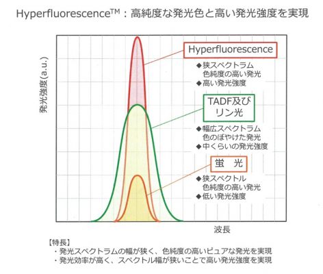
In addition, the Phosphor-Sensitized Fluorescence (PSF) structure, which is attracting attention as a fourth-generation hyperfluorescent material, achieved a low drive voltage (2.5 V), maintained efficiency (minimized roll-off), and a lifetime of LT₈₀ > 1,000 hours at a luminance of 100 cd/m².

Prof. Hatakeyama said that Double Borylation is not just a synthesis technique, but a strategic approach that changes the fundamental concept of OLED material design, and succeeds in improving color purity, efficiency, and lifetime, and is expected to be used in a variety of next-generation applications, including microOLEDs (OLEDoS) for AR-VR, ultra-high color purity smartphone and TV displays, automotive heads-up displays (HUDs), wearables, and transparent displays. 

Device structure, emission spectrum (467 nm, FWHM 17 nm), and CIE coordinates (0.12, 0.12) of ν-DABNA-M-B-Mes OLED (Source: Nature Communications, 2025)

Emission Characteristics of ν-DABNA-M-B-Mes OLED (Source: Nature Communications, 2025)

Changho Noh,  Senior Analyst at UBI Research  (chnoh@ubiresearch.com)

▶OLED Emitting Material Market Tracker Sample

▶2025 OLED Emitting Materials Report Sample

OLED emitting material demand expected to grow to 177 tons by 2028

According to the ‘2024 OLED Emitting Materials Report’ recently published by UBI Research, the total demand for emitting materials in 2024 is expected to be 131 tons, and the demand for emitting materials is expected to be 177 tons by 2028 with an average annual growth rate of 7.9%.

According to the report, as Samsung Electronics applied rigid OLED to its Galaxy A entry-level product, Samsung Display’s rigid OLED shipments, which were previously expected to decrease, increased. Additionally, as the application of OLED to IT devices, including iPad, expands, the demand for emitting materials is expected to increase until 2028.

The size of the OLED emitting materials market is also expected to increase. According to the report, the overall OLED emitting material market is expected to grow from $2.4 billion in 2024 to $2.7 billion in 2028.

Korean panel companies’ OLED emitting material purchases are expected to increase from $1.4 billion in 2024 to $1.5 billion in 2028, and Chinese panel companies’ material purchases are expected to increase from $980 million in 2024 to $1.21 billion in 2028.

‘The 2024 OLED Emitting Materials Report ‘ includes the latest trends in iPad Pro OLED, which recently started production, emitting material structure and supply chain, 8.6G IT line investment trend by panel company, tandem OLED emitting material development trend, and high-efficiency and long-life emitting material development trend, etc.

▶ 2024 OLED Emitting Materials Report Sample Download

The 4th Generation Emitting Material, Hyperfluorescence

Thermally activated delayed fluorescence(TADF), still under development to complement OLED emitting materials insufficient as both fluorescence and phosphorescent materials, takes time to be commercialized at the present stage. Even Kyulux considered the most advanced company in terms of TADF technology hasn’t yet to commercialized TADF dopant suitable for display.

Adachi, CTO of Kyulux said the unprepared TADF host material is an obstacle to the commercialization of TADF, so the full width at half maximum of emitting peak is too wide to be applied to display. To solve this problem, the 4th generation hyperfluorescence is under development to commercialize the TADF material.

<Kyulux CTO Adachi>

Hyperfluorescence aims at having the effect of a phosphorescent material by adding TADF dopant to existing fluorescence host and dopant.

<Hyperfluorescence Effect>

This effect has a structure that can solve both the full width at half maximum of TADF and the low brightness of fluorescence materials as seen in the above figure, Adachi emphasized.

<Hyperfluorescence vs General fluorescence>

As seen in the above photo, Kyulux’s OLED made of general green fluorescence material and OLED made of hyperfluorescence by adding TADF to this material have a distinct difference on the same substrate.

Kyulux’s goal is to commercialize hyper fluorescence by 2017. Its target is PMOLED.

International TADF Workshop Opening

<Source : 2nd International TADF Workshop>

The International Workshop on the third generation of light emitting material technology, TADF (Thermally Activated Delayed Fluorescence) technology, which links first-generation fluorescent material technology and second-generation phosphorescent material technology, will be held at Kyushu University from July 19 to 21, 2017

In order to push the LCD, which is now the flagship product of the display market replacing the cathode-ray tube completely in the market, it is necessary to have a high-efficiency, low-cost OLED that can be used in mid/low-priced products. A solution to solve both high efficiency and low cost depends on the commercialization of retarded fluorescent materials.

Currently, the light emitting materials are classified into red, green, and blue host materials and dopant materials of respective colors. Among these materials, red and green use phosphorescent materials that internal efficiency is theoretically 100%, but blue materials still use fluorescent materials that internal efficiency is only 25%. Due to the limit of blue material efficiency, large OLED panels for TV have a structure in which blue layers are laminated twice, so material cost is very high.

TADF is the material that is being developed to overcome the limitations of current OLED emissive materials.

In the International TADF Workshop, headed by Professor Adachi of Kyushu University, who brought TADF technology to the world for the first time, worldwide experts of third-generation OLED lighting material development gather. Professor Adachi implied that the interest in TADF is getting hotter around the world looking from that 3 years later he published a TADF thesis for the first time in 2012 at Kyushu university approximately 120 papers published worldwide in 2015 and there are more than 200 papers published in 2016.

Professor Adachi said that the meaning of the TADF Workshop this time is to discuss with experts about the current TADF reach and future development.