Posts

AUO's transparent Micro-LED display structure showing a stained glass design at Touch Taiwan 2026, representing its Smart Life Solution transformation.

[2026 Touch Taiwan] “Connecting the World with Light”… AUO Emerges as a Global “Smart Life Solution” Group

AUO, which previously focused on the manufacturing of display panels, has by 2026 completely transformed into a massive “Smart Life Solution Group” encompassing Artificial Intelligence (AI), mobility, and optical communications.

At its core lie Ennostar, the central hub for next-generation optoelectronic integrated solutions; AMS (AUO Mobility Solutions), which leads the automotive business; and ADP (AUO Display Plus), a company specializing in industry-specific customized solutions.

Giant transparent Micro-LED display structure featuring a colorful stained glass pattern at the entrance of the AUO booth at Touch Taiwan 2026

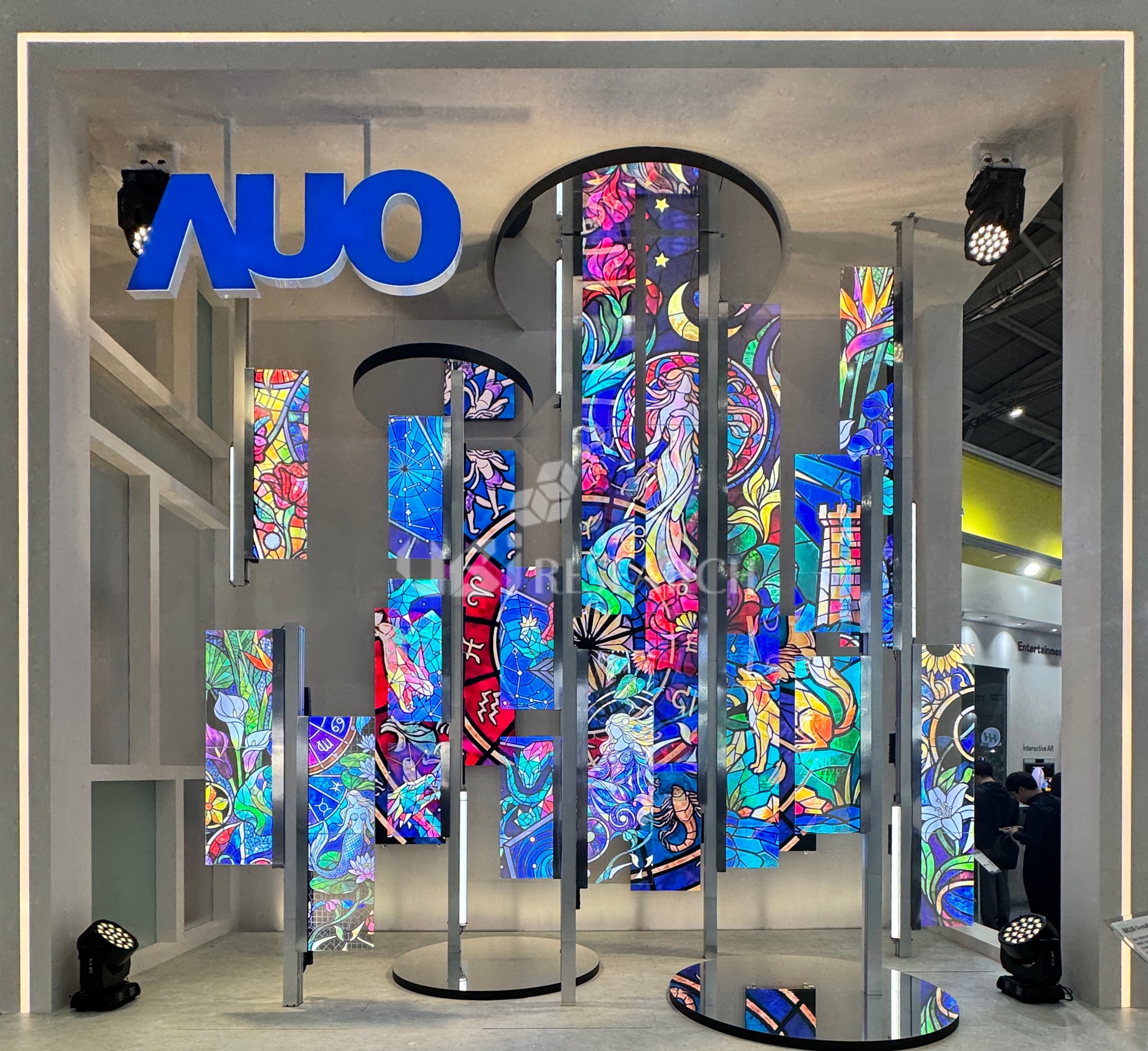
A giant transparent Micro-LED display structure at the entrance of the AUO booth at Touch Taiwan 2026. Featuring a colorful stained glass pattern, it symbolizes AUO’s leap beyond hardware manufacturing into a ‘Smart Life Solution’ group. (Source: UBI Research)

■ Ennostar: The Heart of the Micro-LED Ecosystem, from Upstream to Downstream

Ennostar, the technological foundation of the AUO Group, has established a unique vertical integration system in the Micro-LED field—often hailed as the game-changer for next-generation displays.

• Design and Production: Through in-house design and production of LED epitaxial wafers and chips, Ennostar has internalized the core material technologies essential for next-generation displays.

• Evolution of Packaging and Modules: Moving beyond mere chip production, Ennostar has developed its packaging and module business as a primary pillar, fulfilling its role as a core supply chain partner within the group by providing automotive solutions to its subsidiary, AMS.

■ AMS and ADP: Innovation in Mobility and Smart Spaces

High-performance LED packaging and module solutions produced by Ennostar are elevated into cutting-edge automotive solutions through the subsidiary AMS.

• Smart Cockpit: AMS combines Ennostar’s pixelated automotive LEDs with high-brightness Micro-LED panels to supply “Smart Cockpits”—interfaces for the era of autonomous driving that go beyond simple instrument clusters—to global automakers.

• Customization Services: ADP applies these technological capabilities to medical, retail, and educational displays, diversifying the group’s revenue structure by providing smart space solutions optimized for each industry.

■ “We Sense, We Communicate”: Opening the Arteries of AI Data Centers

The evolution of AUO and Ennostar does not stop here. Under the new motto “We Sense, We Communicate,” both companies are leaping beyond being display manufacturers to become integrated optoelectronic solution providers.

In particular, they are focusing on high-speed data transmission solutions for AI data centers to handle the explosive growth of traffic in the AI era. Ennostar’s compound semiconductor and light source technologies are merging with silicon photonics, evolving into core components that reduce power consumption and maximize data transmission efficiency.

■ Building an Intelligent Ecosystem Beyond Hardware

Analyst Joohan Kim of UBI Research analyzed that “the ability to control ‘light’ that AUO has secured through Ennostar has now moved beyond the purpose of illuminating screens to become the pathway for the flow of AI data.”

As a leader of an intelligent ecosystem that connects everything from the arteries of AI data centers to mobility interfaces—rather than just a panel manufacturer—AUO’s 2026 is shining more brightly than ever before.

Joohan Kim, Senior Analyst at UBI Research (joohanus@ubiresearch.com)

▶101 inch Micro-LED Set BOM Cost Analysis For TVs

▶Industry Trends and Technology of Micro-LED Displays for XR Report

※ This article is produced by UBIResearchNet.

Unauthorized reproduction or citation without source attribution is prohibited.

When quoting, please clearly indicate the source (UBIResearchNet) and provide a link.

Co-Packaged Optics (CPO) packaging technology roadmap showing the integration of Micro-LEDs for AI data centers.

Expanding into new markets through an integrated solution combining Micro-LED and CPO technology

Generative AI has ignited a global race for computing power, with high-speed transmission bottlenecks in data centers emerging as a key obstacle constraining AI infrastructure upgrades. While chip-internal computation speeds have accelerated dramatically, the copper wiring connecting chips cannot keep pace with data transmission speeds due to resistance and heat generation issues. Next-generation ultra-high-speed, ultra-low-power optical interconnect solutions are establishing themselves as the core alternative to traditional copper cable interconnects, offering a new solution to the transmission challenges facing AI computing centers and data centers. Micro-LEDs are gaining attention as the optimal light source to solve this problem and could become a key technology for overcoming the ‘energy barrier’ in AI infrastructure.

In early March, Chinese micro-LED-related stocks saw significant gains. The surge in buying pressure, driven by capital inflows, stems from the rise of micro-LED CPO (Co-Packaged Optics) technology. Recently, micro-LED companies, including those in Taiwan and China, are accelerating development not only in display products but also in the ‘non-display sector’—specifically the optical communication and optical sensor markets.

PlayNitride is strengthening its R&D efforts to develop communication-specific Micro-LED chips capable of high-speed modulation and to convert ultra-high-resolution LEDos technology into arrays for optical interconnects. In January this year, it announced a partnership with Brillink to jointly develop micro-LED-based optical interconnect solutions. AUO is preparing to enter the CPO market for next-generation AI servers by leveraging its display supply chain. It is attempting to establish a vertical integration by combining the micro-LED resources of its subsidiary, LED chip manufacturer Ennostar, with the receiver technology of Tyntek. China’s largest display manufacturer, BOE, has established an 8-inch GaN-on-Si-based Micro-LED mass production system in collaboration with its subsidiary HC-Semitek. Aligned with the Chinese government’s ‘semiconductor self-reliance’ strategy, it is building a low-cost light source supply chain for optical interconnects between AI chipsets.

Co-Packaged Optics (CPO) packaging technology roadmap for high-speed AI data centers

Co-Packaged Optics (CPO) packaging technology roadmap designed to resolve high-speed transmission bottlenecks in data centers. (Source: Micromachines 2025, 16, 1037)

Micro-LEDs are gaining attention as an optimal light source for the following reasons.

  • Ultra-high-speed modulation principle: Smaller micro-LEDs reduce RC delay and allow higher current density, enabling ultra-high-speed modulation bandwidths exceeding several GHz. This facilitates data transmission of several Gbps per pixel.
  • Energy Efficiency: Unlike laser light sources (VCSELs: Vertical Cavity Surface Emitting Lasers), they do not require a resonator structure, resulting in extremely low drive power. Efficiency levels around ~1 pJ/bit could be the only viable alternative to dramatically reduce power consumption in AI data centers.
  • High-density packaging: Thousands of light sources can be directly integrated (monolithic/hybrid integration) onto HBM (High Bandwidth Memory) or GPU dies with pitches in the micrometer range, maximizing data transmission density per unit area.

While existing micro-LEDs for displays focused on color reproduction and brightness, the key for optical interconnect solutions lies in compatibility with semiconductor processes. Moving beyond the traditional 4-inch and 6-inch sapphire wafer methods, the introduction of 8-inch and 12-inch GaN-on-Si (Gallium Nitride on Silicon) processes enables the direct use of existing semiconductor fab equipment. This not only lowers manufacturing costs but also enables ‘Monolithic Integration’—packaging the CMOS driver IC and micro-LED together in a single package—accelerating the commercialization of optical interconnect solutions.

Experts anticipate a future where micro-LEDs transcend being mere ‘screens’ and are recognized as key components determining the performance of AI semiconductors. If the micro-LED industry achieves breakthroughs in two core areas—reducing mass production costs and validating the technical feasibility of optical interconnection application scenarios—micro-LEDs will gradually open new markets beyond consumer electronics displays like smartwatches and AR smart glasses, with significant potential for substantial market expansion.

Namdeog Kim, Senior Analyst at UBI Research (ndkim@ubiresearch.com)

▶Pre-register for Display Korea 2026

▶101 inch Micro-LED Set BOM Cost Analysis For TVs

▶Industry Trends and Technology of Micro-LED Displays for XR Report

※ This article is produced by UBIResearchNet.

Unauthorized reproduction or citation without source attribution is prohibited.

When quoting, please clearly indicate the source (UBIResearchNet) and provide a link.