Posts

TCL CSOT's 163-inch X11H Max Micro-LED TV representing the company's push for mass adoption.

Breaking the KRW 100 Million Barrier?” TCL CSOT’s Bold Bet on Micro-LED Mass Adoption

Micro-LED, the pinnacle of “self-emissive” display technology where each pixel generates its own light, is finally shedding its laboratory skin and attempting to enter the living room. At the forefront is TCL CSOT, which has thrown down a bold technical roadmap in a market once considered the exclusive domain of Samsung Electronics. We analyze their three-stage evolution—from CES 2025 through the recent DTC 2025 to the upcoming CES 2026—through the lens of display engineering.


1. [CES 2025] The 10,000-Nit Shock: Pushing the Limits of Inorganic Elements

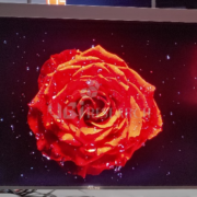
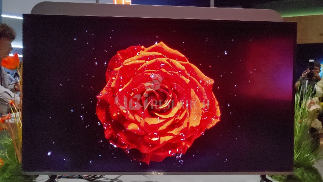
At CES 2025, TCL CSOT’s 163-inch Micro-LED TV, the ‘X11H Max’, injected significant technical tension into the industry. It wasn’t just about the size; the device achieved a staggering peak brightness of 10,000 nits by individually controlling approximately 24.88 million inorganic RGB chips at the pixel level. This was a landmark event that redefined the standards of “super-gap” picture quality, using the durability of inorganic materials to directly overcome the brightness degradation and burn-in issues inherent in organic-based OLEDs.

TCL CSOT's 163-inch X11H Max Micro-LED TV and pricing unveiled at CES 2025 (Source: TCL CSOT)

TCL’s 163-inch Micro-LED TV ‘X11H Max’ achieving 10,000 nits brightness, surpassing the limits of inorganic devices. (Source: TCL CSOT)

2. [DTC 2025] Technical Maturity in Driving Algorithms and Grayscale Expression

The key takeaway from DTC 2025 (TCL Global Display Tech Ecosystem Conference) was the “evolution of internal substance.” TCL addressed the chronic challenge of Micro-LEDs—color distortion in low-light areas—through its proprietary ‘Hybrid PWM+PAM Driving Architecture.’ This method, which sophisticatedly combines Pulse Amplitude Modulation (PAM) and Pulse Width Modulation (PWM), achieved a 24-bit color depth. It demonstrated technical maturity by perfectly resolving the shapes of objects even in pitch-black darkness through 16.77 million steps of grayscale.

TCL CSOT's 219-inch 36:9 ultra-wide Micro-LED display showcased at the exhibition (Source: TCL CSOT)

A 219-inch ultra-large Micro-LED display supporting 98% DCI-P3 color gamut and 120Hz refresh rate. (Source: TCL CSOT)

3. [CES 2026 Outlook] Crushing the “100 Million Won” Wall via Mass Transfer Innovation

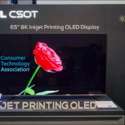
At the upcoming CES 2026, TCL is expected to move beyond technical posturing and place a practical bet on “price destruction.” Experts predict that TCL will drastically lower the production cost of 100-inch+ models by significantly increasing the yield of the Mass Transfer process—the method of moving millions of microscopic chips onto a substrate. In particular, process efficiency linked with Inkjet Printing (IJP) technology is projected to be the detonator that pulls down Micro-LED TV prices, once exceeding hundreds of thousands of dollars, to the tens of thousands range (approx. 50–80 million KRW).

While past Micro-LEDs were merely “expensive display pieces densely packed with small LEDs,” today’s TCL CSOT is attempting to democratize “nanosecond-level response speeds” and “infinite contrast ratios” by perfectly grafting semiconductor micro-processes onto displays. CES 2026 will serve as the “technological singularity” where Micro-LED moves beyond being a luxury for the ultra-wealthy to become the new standard for premium home appliances.

Joohan Kim, Senior Analyst at UBI Research (joohanus@ubiresearch.com)

▶2025 Micro-LED Display Industry and Technology Trends Report

※ This article is produced by UBIResearchNet.
Unauthorized reproduction or citation without source attribution is prohibited.
When quoting, please clearly indicate the source (UBIResearchNet) and provide a link.

eatured image for TCL CSOT’s T8 Gen-8.6 inkjet-printed OLED line indicating equipment ordering and 2027 mass-production target (Source: TCL CSOT, UBI Research)

CSOT T8 8.6G IJP OLED Project Nears Key Equipment Orders…Despite Scheduling Variables, Mass-Production Target Remains Intact

TCL CSOT inkjet-printed OLED monitor panel on display (Source: TCL CSOT)

Demonstration of TCL CSOT’s IJP OLED monitor panel (Source: TCL CSOT)

TCL CSOT’s T8 project, the world’s first Gen 8.6 inkjet printing (IJP) OLED mass-production line, has officially entered the equipment-ordering phase. Following a series of IJP OLED and oxide TFT roadmap disclosures at DTIC 2025 that demonstrated the company’s technical readiness, the project is now showing visible progress on the investment timeline as well.

According to industry sources, orders for core T8 equipment, including inkjet printing systems and deposition tools, are scheduled to begin in December 2024. Inkjet printing, the central platform of the T8 process, determines panel quality, yield, and material utilization; the tool alone is said to account for more than half of the total investment. CSOT is currently engaged in detailed price and specification negotiations with major tool suppliers, while aiming to complete all remaining equipment orders by February 2025. However, with key tool prices trending higher than initially expected, the pace of early investment execution may be adjusted.

CSOT plans to bring in the first batch of equipment for the T8 line in October 2026, though there is a high likelihood that actual delivery could slip toward the end of 2026. Several tool categories still require mass-production-level validation, and negotiations with the inkjet equipment supplier may take longer than anticipated. Even so, the company is maintaining its official target of beginning mass production in the fourth quarter of 2027. Internally, CSOT is said to be preparing mitigation measures to ensure that a 2–3 month delay in tool delivery does not materially impact the overall project schedule.

The strategic significance of the T8 project extends well beyond the addition of a new production line. Inkjet-printed OLED structurally overcomes the process constraints of the conventional FMM (Fine Metal Mask) approach for large-size panels, offering advantages such as material utilization above 90 percent, elimination of large-mask issues, and strong scalability toward high resolution. T8 is designed as a multi-product platform spanning 14–17-inch notebooks, 27–32-inch monitors, and 65–77-inch TVs. Once mass production stabilizes, the T8 line is expected to reshape price-competition dynamics across the IT, monitor, and TV markets.

Junho Kim, Analyst at UBI Research (alertriot@ubiresearch.com)

▶ China Trends Report Inquiry

※ This article is produced by UBIResearchNet.
Unauthorized reproduction or citation without source attribution is prohibited.
When quoting, please clearly indicate the source (UBIResearchNet) and provide a link.

TCL CSOT announces 8th generation inkjet OLED investment plan at K-Display 2025, highlighting Panasonic printing equipment

TCL CSOT to announce investment in 8th generation OLED inkjet production line soon_ Inkjet printing equipment expected to be supplied by Panasonic

TCL CSOT showcases 8th generation inkjet OLED technology and breakthroughs at K-Display 2025

TCL CSOT’s latest inkjet OLED technology presentation at K-Display 2025 (Source: TCL CSOT)

At the business forum of K-Display 2025, held from August 6-9, China’s TCL CSOT said it will announce its investment plans for an eighth-generation inkjet OLED production line. The project, dubbed the “T8 Project,” is planned to begin trial production in June 2027, with equipment delivery targeted for September 2026. The initial production capacity is expected to be 15,000 sheets per month in the first phase. The investment is seen as a significant move to challenge the dominant position of South Korean companies in the large OLED panel market.

 The Inkjet Printing method adopted by TCL CSOT has a number of advantages over the Vacuum Deposition method currently used for large OLED production.

  • Cost and energy efficiency: The process can be completed in a low vacuum environment, significantly reducing equipment costs and energy consumption.
  • Material utilization: Since the organic material is ‘printed’ directly onto the substrate, there is less material waste, resulting in high material utilization.
  • Large substrate production efficiency: It is especially economical for large TV panels such as 65-inch and 77-inch.

One of the main technical challenges with inkjet OLEDs has been the lifetime of blue OLEDs, but TCL CSOT has made significant improvements. The company says its blue lifetime, which was just 40 hours in 2020, is now 400 hours, a tenfold improvement. In addition, the resolution has exceeded 350 PPI, which can meet the needs of high-performance tablets and laptops; the aperture ratio has been increased to three times that of conventional FMM (Fine Metal Mask) OLEDs to reduce power consumption; and the size of blue subpixels has been reduced to be similar to red and green, improving display quality.

Meanwhile, the printing equipment for the 8th generation OLED inkjet line is likely to come from Panasonic Production Engineering. Panasonic Production Engineering announced at SID 2025 that it has developed an 8.5-generation machine with a 1 pL (picoliter) inkjet head and 350 ppi resolution. The machine achieved an accuracy of 4.6 µm, exceeding the target accuracy of 5.8 µm, demonstrating the possibility of stable mass production of large substrates. The expected equipment configuration will consist of a Hole Injection Layer, Hole Transport Layer, and printing equipment for RGB pixel printing, as well as equipment for tandem OLEDs.  Panasonic’s equipment enables the production of high-resolution displays through high-frequency jetting (20 kHz) and droplet volume control as fine as 1.0 pL, which are key technologies for improving the productivity of the inkjet process. The company also reports that production stability is enhanced through a sophisticated system that compensates for thermal deformation and micro-alignment errors.

Inkjet OLED technology still has many challenges to overcome. While current technology has improved device lifetime, there is ongoing debate about whether it has achieved sufficient lifetime for commercialization. There are also limitations that make it difficult to implement tandem structures for high brightness and low power consumption. These challenges are directly related to the yield of the production line and require continuous technology development for successful mass production of inkjet. Nevertheless, TCL CSOT’s technological advancements show that inkjet OLEDs are getting closer to reality.

If TCL CSOT’s eighth-generation inkjet OLED investment materializes, it will pose a direct challenge to the mid- to large-sized OLED market dominated by South Korea’s Samsung Display and LG Display. Currently, these two companies rely on a costly vacuum deposition process, which keeps OLED TV prices high. Mass production using inkjet technology can bring cost competitiveness, which will significantly reduce the price of OLED TVs and increase market penetration. Furthermore, the technology is expected to impact not only the TV market, but also the laptop, tablets, and professional monitor markets. Inkjet technology can become an important steppingstone for China’s display industry to secure technological leadership in the OLED field, following LCD.

Changho Noh, Senior Analyst at UBI Research  (chnoh@ubiresearch.com)

▶ China Market Trend Report Inquiry

TCL CSOT Establishes Investment Plan for 8.6-Generation Inkjet Printing OLED Line Worth RMB 20 Billion

Plans for 8.6G OLED Line Construction by Panel Makers

Plans for 8.6G OLED Line Construction by Panel Makers

Monthly Production Capacity of 45K; Equipment Installation Targeted for End of 2026

According to UBI Research’s China Market Trend Report, Chinese display company TCL CSOT (China Star Optoelectronics Technology) is planning to construct a new 8.6-generation (2290x2620mm) OLED line at the T8 site near its existing T9 OLED line in Guangzhou. This investment will be based on inkjet printing technology, with a Step 1 investment fund scale of approximately RMB 20 billion (approximately KRW 3.8 trillion).

The T8 site was initially intended to be converted for a solar project, but that plan has been put on hold, and the site will now be used for its originally planned OLED production line. The T8 project is designed to consist of two 8.6G OLED lines with a total monthly production capacity of 45,000 substrates (45K), and the initial investment will be made for one line.

The investment schedule for the T8 line includes an official announcement in July 2025, groundbreaking in October, and the start of equipment installation by the end of 2026. The general manager of the project has been appointed as Linpei (林佩), and the core inkjet process technology is being led by a Korean expert.

Inkjet printing technology is known for its approximately 30% lower equipment investment cost compared to the traditional mask-based deposition method. For example, Samsung Display is investing around KRW 4 trillion to build an 8.6-generation OLED line for IT applications (15K per month) at its A6 site in Asan, Chungcheongnam-do, based on the conventional deposition process. In contrast, TCL CSOT plans to adopt inkjet printing technology to secure a monthly production capacity of 45K at the 8.6-generation level, with an initial investment of RMB 20 billion.

Han Changwook, Executive Vice President of UBI Research, commented, “Inkjet OLED still faces technological challenges in brightness, lifespan, large-area uniformity, and yield. Nevertheless, China is positioning this differentiated technology from traditional deposition as a next-generation growth driver and, under strategic government support, is preparing for full-scale mass production. Through investments in inkjet technology by TCL CSOT and ViP (Visionox intelligent Pixelization) by Visionox, China is pushing ahead with the first mass production of large-area OLEDs, aiming to secure technological leadership.”

As demand for IT displays is expected to grow, it remains to be seen whether the commercialization of inkjet technology in large-area OLEDs will determine future market leadership.

Changwook HAN, Executive Vice President/Analyst at UBI Research (cwhan@ubiresearch.com)

▶ China Market Trend Report Inquiry

SID 2025, TCL exhibits inkjet OLEDs from 6.5 inches to 65 inches… Will mass production shake up the display market?

At the SID 2025 Display Week, TCL showcased various sizes of inkjet OLED products. The inkjet method is considered to be a technology that is advantageous in reducing material costs compared to the vacuum deposition method due to its high utilization efficiency of luminescent materials. TCL officially announced the mass production of a 21.6-inch 4K inkjet OLED professional display in November 2024, and is currently considering investment for mass production.

At this exhibition, TCL showcased a 6.5-inch inkjet OLED display for smartphones, which provides a high resolution of 360ppi based on real stripe, which is equivalent to approximately 460ppi based on pentile. In addition, a variety of product lines were exhibited, including a 14-inch oxide TFT-based OLED notebook panel with a 2.8K resolution (243ppi), a 27-inch OLED monitor with 4K 120Hz specifications, and a 65-inch OLED TV display with 33 million pixels and 8K 120Hz.

TCL, 6.5” Smartphone

TCL, 6.5” Smartphone

TCL, 14” Notebook PC

TCL, 14” Notebook PC

TCL, 27” Monitor

TCL, 27” Monitor

The 65-inch product maintains 99% of the DCI-P3 color gamut even in low-gradation, and has applied technology that doubles the utilization of light-emitting materials and reduces blue light by 50%. This is evaluated as a significant technological breakthrough in the large-scale and commercialization of inkjet OLED.

TCL 65” 8K TV

TCL 65” 8K TV

With a full lineup from 6.5 inches to 65 inches, TCL has shown confidence that inkjet OLED technology can be applied to all product lines from mobile to TV. Up to now, Chinese OLED panel manufacturers have focused on production based on technologies first verified by advanced companies, but inkjet OLED is the first technology that China has led in mass production. The success of this technology can be an opportunity for Chinese panel manufacturers to leap forward in both technology and production.

However, OLED using vacuum deposition method is continuously improving brightness and lifespan through tandem IT OLED structure or multi-stack TV OLED structure, and inkjet OLED still has the task of not only securing productivity but also reducing this performance gap.

Chang Wook HAN, Executive Vice President/Analyst at UBI Research (cwhan@ubiresearch.com)

▶2025 Small OLED Display Annual Report Sample

▶2025 Mid-to-Large OLED Display Annual Report Sample

[CES 2023] TCL CSOT 65″ 8K Inkjet Printing OLED

#Inkjetprinting #TCLCSOT #CES2023

▶2023 OLED KOREA
https://oledkoreaconference.com

▶ UBI Research website
https://ubiresearch.com/en/

▶If you are curious about the latest news related to OLED?
https://en.olednet.com/

▶Business, display report inquiry
marketing@ubiresearch.com
+82-2-577-4391

QNED (quantum dot nano-rod LED) structure and core technology

Samsung Display research center is accelerating the development of QNED as the next-generation display following OLED.

The reason Samsung Display is developing QNED as part of its large-size display business is that it is the only display that can produce the image quality that Samsung Display’s biggest customer, Samsung Electronics, can satisfy.

Samsung Electronics’ TV business direction, which has the world’s No. 1 TV market share, is to use QD to make color gamut better than OLED, and to use a display that can maximize HDR performance with high luminance and excellent gradation characteristics on a bright screen.

The only display that can satisfy the needs of Samsung Electronics is QNED.

QNED is a self-luminous display and because it uses QD, it has the best color gamut, HDR, luminance, contrast ratio, and motion blur, etc., and is a product expected by Samsung Electronics.

It can be confirmed by the structure that QNED is the display with the best characteristics. QNED consists of a pixel layer with a nano-rod LED on the TFT structure of 3T1C used in large OLEDs, and a color conversion layer consisting of QD and CF (color filter) on top.

In OLED, electrodes (cathode and anode) and electrode line for transmitting a signal to a pixel are located above and below the light emitting material, whereas in QNED, both the signal transmitting electrode (pixel electrode) and electrode line are located on the same plane. In addition to the pixel electrode, the QNED additionally includes a reflective electrode to increase light output efficiency. The pixel electrode serves as an alignment electrode for aligning the nano-rod LED.

< QNED section structure >

< QNED pixel structure >

< QNED pixel planar structure >

Looking at the planar structure of a QNED pixel, a plurality of pixel electrodes are connected in series in one pixel, and a nano-rod LED is positioned between the pixel electrodes. The pixel electrode is on the pixel wall (PW) formed of an insulating material, and each pixel is surrounded by a bank (BNK) to separate regions.


The core technology of QNED is driving technology and sensing technology.

The driving technology includes a driving technique for aligning nano-rod LEDs and a driving technique for uniformly controlling pixels that may have a deviation in the number of nano-rod LEDs. The alignment circuit includes switching elements for each pixel, and the switching element applies an alignment signal to the pixel. The alignment state of the nano-rod LED is determined depending on which alignment signal is given to each pixel.

< Drive circuit for alignment >

< Sensing transistor for checking alignment >

The most important driving technology is a technology that supplies current to each pixel so that the luminance can be uniform across the entire screen even if the number of nano-rod LEDs per pixel is different. It is a method of controlling each pixel based on the data read from the sensing transistor.

[QNED Technology Completion Analysis Report] details the sensing transistor, sensing wiring, and sensing signals that can check the nano-rod LED alignment status on the panel.


As sensing technology, there are sensing technology (sensing transistor) designed inside QNED and sensing technology used in QNED manufacturing. The sensing technology used to manufacture QNEDs is inherent in inkjet systems. There are three sensing technologies in the inkjet system: the number of nano-rod LEDs in the ink and the viscosity analysis of the solvent, the analysis of the number of nano-rod LEDs sprayed on the panel, and the analysis of the nano-rod LED alignment state.

< Inkjet system configuration >

QNED has already proven that 4K 65 inches can be driven two years ago. Samsung Display is concentrating on finishing work to secure the screen uniformity of QNED.

[28TH FINETECH JAPAN] JDI and JOLED, announced Strengthening Cooperation for Mid-sized OLED Market

At the 28th FINETECH JAPAN held in Tokyo, Japan from December 5 to 7, 2018, JDI and JOLED announced that they would intensify their cooperation in order to target the middle-sized OLED market.

JDI announced that it will actively promote JOLED’s solution process OLED to medium-sized OLED markets such as industrial display markets or automotive display markets through its own design know-how, production infrastructure, and sales channels,.

In particular, JDI announced that it will provide new value to next-generation automotive fields along with JOLED such as support for safety such as electronic mirrors and displays for A/B pillars, new interface functions, movie appreciation using 4-8K displays, and the displays that are harmonized with interior design such as curved surfaces and big screens.

JDI and JOLED also shared booths for exhibition. JOLED introduced 21.6-inch FHD OLED monitors for e-sports and medical applications. In addition, it introduced a number of medium-sized OLEDs such as 12.3-inch HD OLED for automobiles, 12.2-inch FHD flexible OLED, 27-inch 4K OLED for home interior, and 21.6-inch 4K flexible OLED with cylindrical form. It also showcased large OLEDs such as 54.6 inch 4K OLED.

On the other hand, JOLED announced in July, 2018 that it would open its Nomi office for mass production of solution process OLED. Based on 5.5 generation glass substrates, Nomi has production capacity of 20,000 glass substrates per month and plans to mass-produce in 2020.

JOLED raised 47 billion yen to spur solution process OLED business for automobiles.

JOLED, the world’s first to successfully commercialize solution process OLED products, announced that it had raised a total of 47 billion yen as a third-party capital increase.

According to JOLED, Denso will invest 30 billion yen, Toyota Tsusho 10 billion yen, Sumitomo chemical 5 billion yen and SCREEN Finetech Solutions 2 billion yen. JOLED is known to cooperate with Denso to develop automotive displays and Sumitomo chemical to develop OLED materials for solution process.

In particular, Denso has been mainly using TFT-LCD for automotive displays, but it is expected to lead the development for applying lightweight and easy-to-shape OLED to automobile interior through this investment.

It is expected that this funding will accelerate the establishment of production system for the mass-production of JOLED’s solution process OLED. JOLED announced on July 1 that it would set up a “JOLED Nomi Office” in Nomi-city, Ishikawa, and aim to operate in 2020.

Major production products are medium-sized (10 to 32-inch) solution process OLEDs that will be used for cars or high-end monitors. Also, Toshiaki Arai, chief technologist of JOLED announced that they would target the middle-sized OLED market with solution process OLED, at the 2018 OLED Korea conference hosted by UBI Research in March.