China’s WSMT Attracts $14 Million Investment…. Technology Competition with JBD in the MicroLED Market is in Full Swing

Westlake Smokey Mountain Technology (WSMT), headquartered in Hangzhou, China, has recently successfully attracted a pre-series A investment of approximately RMB 100 million (approximately US$14 million). The investment was made by Shenzhen Capital Group (SCGC), Ivy Capital, Moganshan Fund, Lenovo Capital & Incubator Group, and others, suggesting that WSMT has entered into full-scale preparations for Micro-LED mass production.
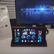
WSMT is a company developing Micro-LEDs with a vertically stacked structure of RGB elements based on technology from Westlake University (Westlake University). Unlike the conventional RGB separated structure, this technology vertically stacks red (R), green (G), and blue (B) LEDs on a single chip, fundamentally solving the problem of pixel alignment accuracy, and is regarded as an advantageous structure for realizing high-resolution small displays.
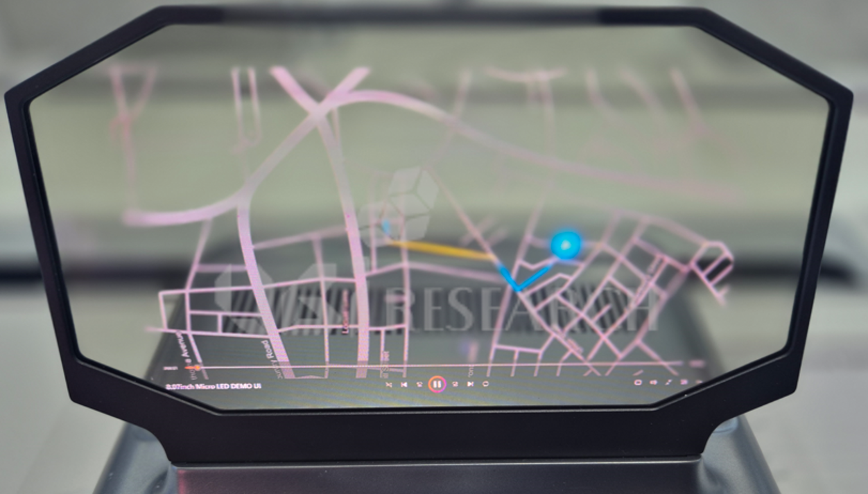
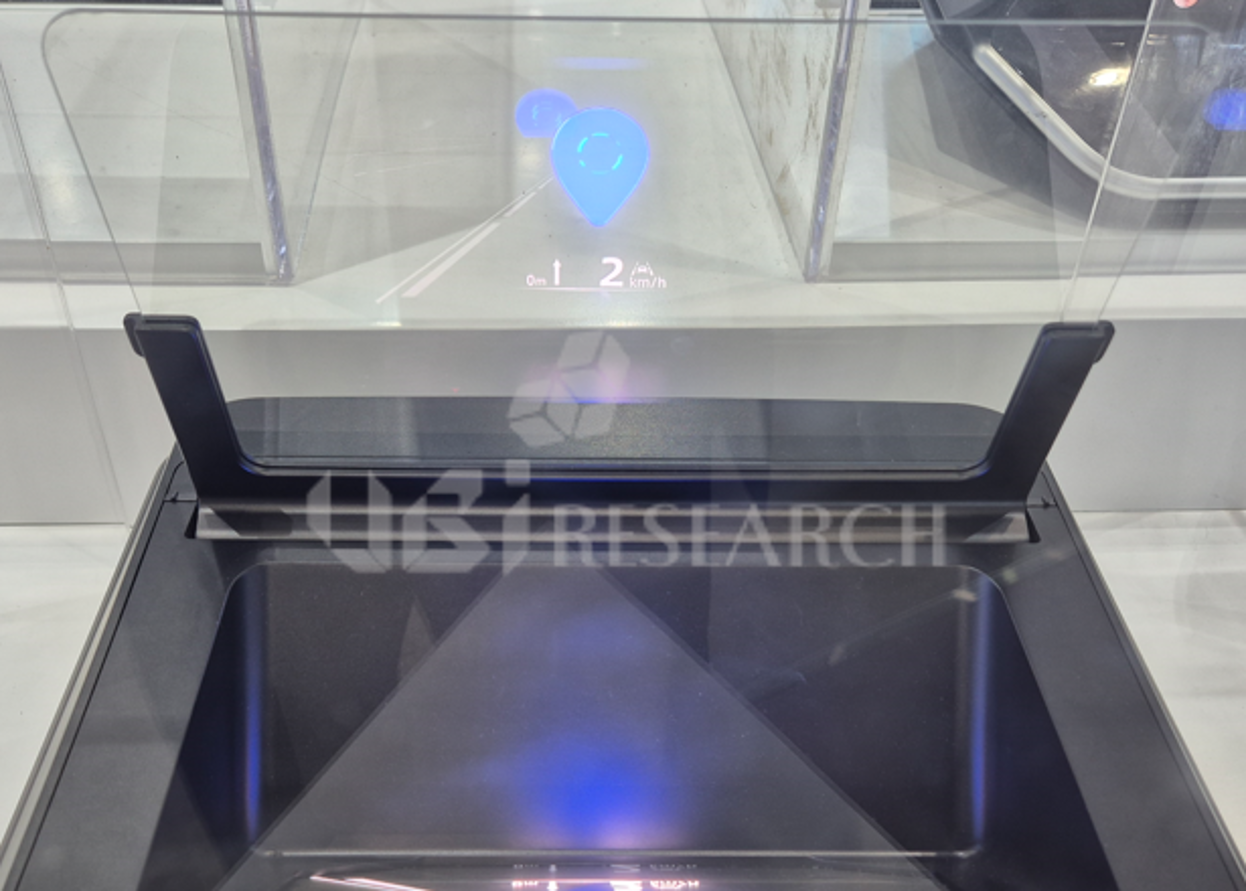
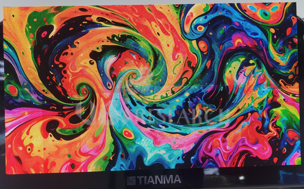
The company is currently building an epi-wafer production line for Micro-LEDs in Huzhou, Zhejiang Province, which is expected to be in production by the end of 2025.WSMT emphasizes that this technology will enable ultra-high resolution of over 5,000dpi, a lifetime of over 100,000 hours, low power (<50mW, 10K nits standard) The company emphasizes that this technology can be used not only for microdisplays for AR/VR, but also for scalability of large-area displays of 8 inches or larger.
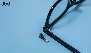
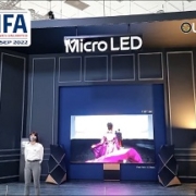
At the same time, Jade Bird Display (JBD), located in Shenzhen, China, also started sample shipments of its “Phoenix series” of RGB vertically stacked micro-LED microdisplays. ㎛JBD also plans to mass produce 0.3-inch, 4K resolution products by the end of 2025.
JBD has until recently secured tens of millions of dollars in funding through the A4 strategic investment round and A3 round, with major global companies such as Alibaba, Samsung, BYD, and Geely as major investors. In particular, JBD is working with BYD on the joint development of Micro-LED displays for vehicles. Currently, JBD is operating a $92 million mass production line in Hefei with a total capacity of 120 million 0.13-inch panels per year.
WSMT and JBD are both developing Micro-LED technology based on the vertically stacked RGB structure, but WSMT, as a research-oriented startup, is emphasizing the perfection of the technology and the potential for large-area deployment, while JBD is securing an advantage in terms of commercialization and speed of market entry.
The competition between WSMT and JBD is part of China’s strategy to secure technology leadership in the global MicroLED ecosystem. The competition between WSMT and JBD can be interpreted as part of China’s strategy to secure technology leadership in the global MicroLED ecosystem, and is expected to influence the strategic choices of Apple, Meta, Samsung Electronics, and others in the future.
Joohan Kim, Analyst at UBI Research (joohanus@ubiresearch.com)
 UBI Research’s Micro Display Report


 UBI Research website