Sunic System to Supply Mass-Production Deposition Equipment for China’s Accelerating 12-Inch OLEDoS Investment, Signing Supply Agreement with Anhui Hongxi Weixian Technology

Metaways’ Wholly-Owned Subsidiary (12-inch OLEDoS) Officially Topped Out! Sunic System’s equipment is set to be installed here. (Source: Metaways)
Sunic System, a Korean OLED deposition equipment company, has signed a contract to supply deposition equipment for mass production of Micro OLED (OLED on Si, OLEDoS) displays with Chinese microdisplay manufacturer Anhui Hongxi Weixian Technology Co., Ltd. (安徽宏禧微显科技有限公司). This is interpreted as evidence that the ultra-high resolution microdisplay market for XR/AR is moving beyond technology validation into the stage of building commercial mass production infrastructure.
According to Sunic Systems’ disclosure, the contract was signed on February 4, 2026, with a contract value of KRW 20.5758 billion (USD 14.2M). The contract period runs from February 4, 2026, to September 15, 2026, with delivery dates subject to mutual agreement between the parties. Payment terms stipulate 50% within 30 days after contract signing, 40% prior to shipment, and 10% via T/T after installation and inspection completion.
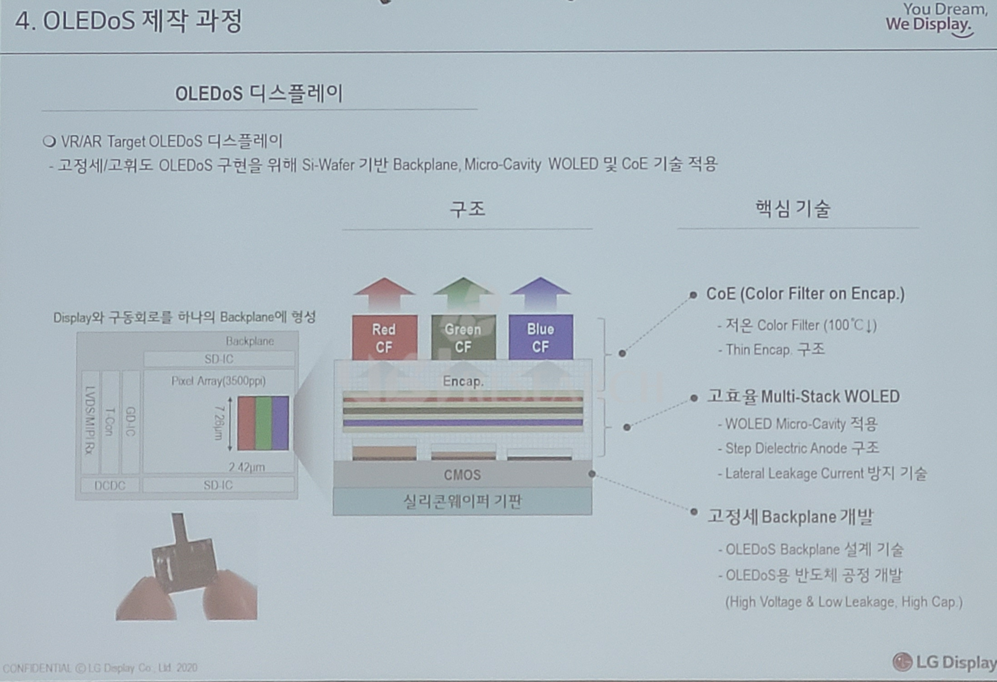
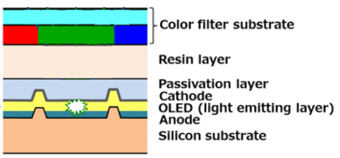
OLEDoS is a technology that deposits organic materials onto a silicon wafer-based backplane to achieve ultra-high resolution, high brightness, and low power consumption. It is gaining attention as a core display for next-generation devices such as XR/AR headsets and smart glasses. Particularly in OLEDoS manufacturing, the deposition process determines critical quality indicators (CTQs) like yield, uniformity, and stack stability. Therefore, the order for ‘mass-production deposition equipment’ is seen as a signal reflecting the customer’s commitment to transitioning their production system.
The background to this contract includes the investment by Anhui Hongxi, a subsidiary of the Metaways (Zhejiang Hongxi Technology) Group, and the local Chinese government in establishing a 12-inch OLEDoS production base. Metaways, as the group’s parent company, has been advancing OLEDoS technology and business, while Anhui Hongxi Micro-Display/Weixian is interpreted as the structure materializing through agreements with the local government in Anhui Province and project promotion entities. According to the publicly announced Chinese announcement, the company signed a 12-inch OLEDoS project investment agreement with the Chuzhou City government in Anhui Province, China, in August 2024. The first-phase investment amount was stated as 2 billion yuan. The agreement’s target goals include an annual production capacity of 72,000 12-inch wafers (72K) and an annual production value of 3 billion yuan, clearly indicating this is a CAPEX investment for mass production, not merely a pilot project. Chuzhou is a city in Anhui Province, and the project is reportedly being pursued within a local high-tech industrial park.
According to UBI Research’s analysis, the flow of actual equipment orders following the establishment of this ‘government-agreement-based CAPEX framework’ demonstrates that the Chinese OLEDoS ecosystem is rapidly transitioning and expanding to 12-inch-based OLEDoS, alongside the swift introduction of core process (deposition) equipment.
From Sunic System’ perspective, this contract secures an additional reference for mass-production equipment for OLEDoS used in XR/AR. OLEDoS is an area with high panel manufacturing difficulty, where process stability, yield, and material/stack optimization act as entry barriers. Consequently, securing mass-production equipment orders not only contributes to short-term sales but can also serve as leverage for future additional CAPEX (line expansion/process scaling) and securing new customers.
This case is seen as a signal that China’s OLEDoS ecosystem is materializing through large-scale line construction based on government agreements and the introduction of core process equipment. Simultaneously, it demonstrates that Korean equipment suppliers are securing meaningful supply references within this trend.
Changho Noh, Senior Analyst at UBI Research (chnoh@ubiresearch.com)


※ This article is produced by UBIResearchNet.
Unauthorized reproduction or citation without source attribution is prohibited.
When quoting, please clearly indicate the source (UBIResearchNet) and provide a link.


 China Trends Report Inquiry


