Demonstrating the suitability of PSF materials for hybrid processes
A joint research team from Beijing Summer Sprout Technology and Guangdong Juhua Printed Display Technology announced at ICDT2026 that they had achieved efficiency, color purity, and lifetime on par with vacuum thermal evaporation (VTE) devices by spin-coating phosphorescent-sensitized MR-TADF (hereinafter PSF) materials. This research is drawing attention as it aligns with the technological initiatives of TCL CSOT, which is currently pursuing the mass production of large-area RGB OLEDs based on inkjet printing.
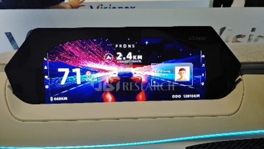
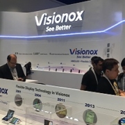
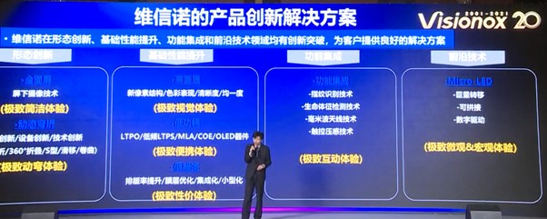
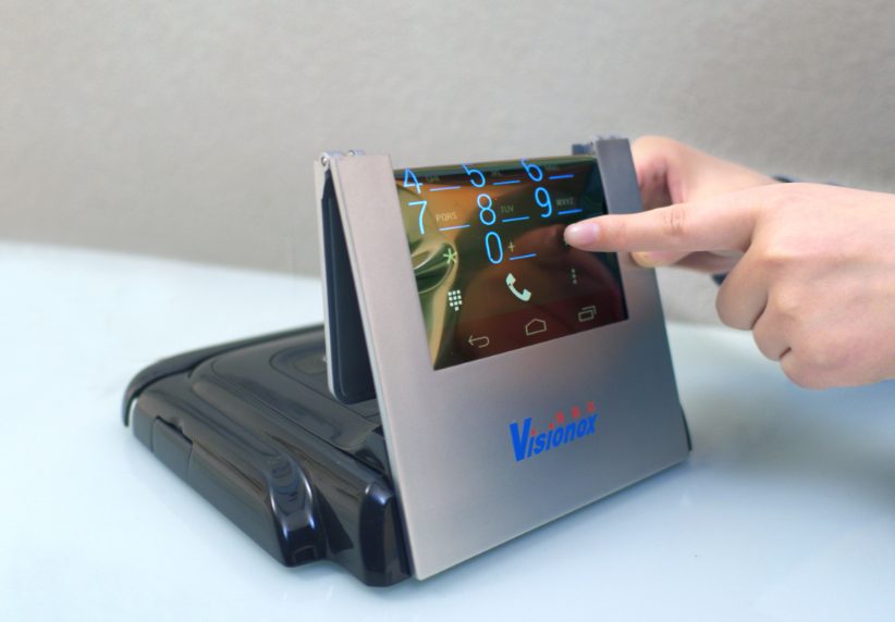
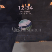
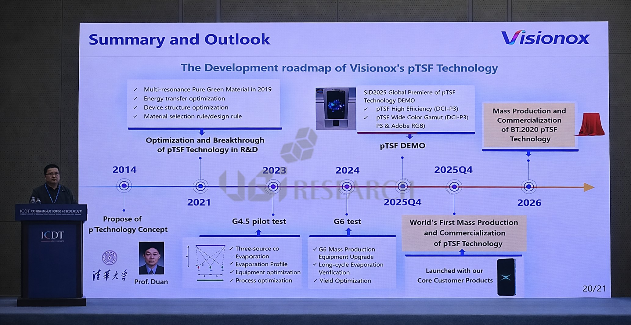
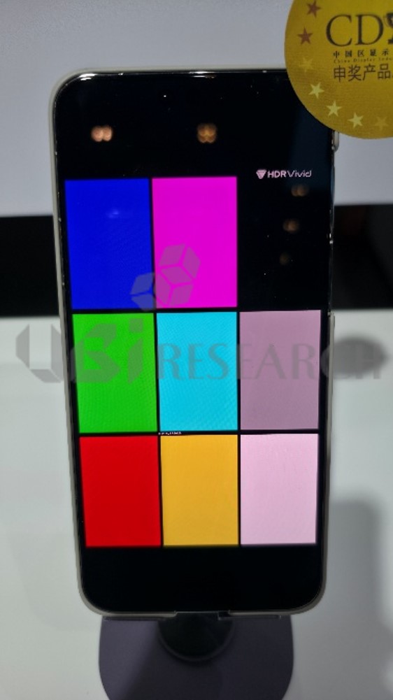
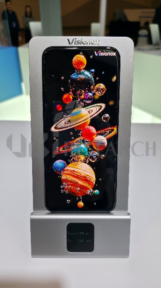
PSF has already been validated as a technology capable of simultaneously achieving high efficiency, high color purity, and low roll-off in vacuum-deposited devices, and Visionox has begun applying PSF materials to AMOLED panels for smartphones.
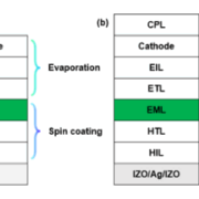
The device structure adopted in this study is a hybrid method in which the emissive layer (EML) is formed by spin coating, while the electron transport layer (ETL), electron injection layer (EIL), cathode, and capping layer (CPL) are stacked via vacuum deposition. The research team used a process sequence in which the three hole-side layers were formed via spin coating, followed by substrate pretreatment with UV ozone treatment and baking at 230°C. After applying the EML via spin coating, the remaining layers were completed via vacuum deposition. This is a practical approach that focuses on the EML’s luminous efficiency and color purity while enhancing mass-production feasibility.
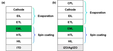
Structure diagram of a solution-processed OLED utilizing a hybrid process
The PSF device developed by the research team achieved a current efficiency of over 200 cd/A at 1,000 nits. This performance is on par with both existing polymer-based solution-processed devices and vacuum thermal evaporation (VTE) devices. The roll-off characteristics were also found to be virtually identical to those of VTE devices. Depending on the composition, the color gamut satisfied 100% DCI-P3 and 95% or more of BT.2020. The device demonstrated a lifespan up to 170% longer than that of a standalone phosphorescent device.
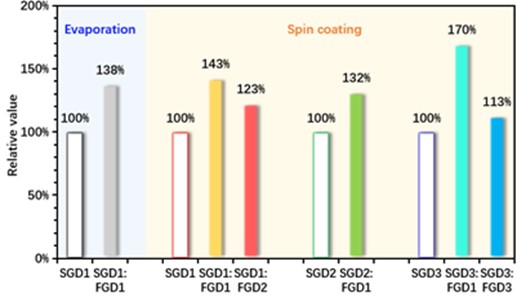
Operational lifetime (LT95) comparison graph demonstrating the enhanced lifespan of the PSF solution-processed device compared to phosphorescent OLED devices.
After more than 10 years of research, TCL CSOT began small-scale mass production of inkjet-printed OLED panels at its 5.5-generation line in Wuhan in November 2024 and aims to begin shipping 27-inch 4K 120Hz inkjet OLED panels for monitors in July 2026. Construction began in October 2025 on the Guangzhou T8 8.6-generation fab, where approximately $4.15 billion is being invested to build a dedicated inkjet OLED line with a monthly capacity of 22,500 panels, with mass production targeted for 2027. The key reason TCL CSOT chose the inkjet process is to enhance product competitiveness by directly applying light-emitting materials to RGB pixels without an FMM (Fine Metal Mask), thereby increasing material utilization to over 90% and reducing equipment investment costs by approximately 30% compared to VTE.
Spin coating and inkjet printing both fall within the category of solution-based processes; however, inkjet printing entails a higher level of process complexity than spin coating due to its pixel-level selective deposition. While the intrinsic challenges of the inkjet process—such as deposition uniformity, drying control, and jetting stability—must be addressed independently, a material-level basis has been established demonstrating that PSF molecular materials can maintain high efficiency, high color purity, and low roll-off in solution.
The results of the hybrid process hold value as data directly transferable to a fab environment. It remains to be seen whether the mass production of PSF-based, low-cost inkjet OLED panels will become a cost-driven innovation originating from China that disrupts the FMM-process-based OLED supply structure.
Changho Noh, Senior Analyst at UBI Research (chnoh@ubiresearch.com)
 2026 Medium & Large Size OLED Display Annual Report
2025 OLED Emitting Materials Report Sample
※ This article is produced by UBIResearchNet.
Unauthorized reproduction or citation without source attribution is prohibited.
When quoting, please clearly indicate the source (UBIResearchNet) and provide a link.


 China Trends Report Inquiry